Lab 2: Multiplexed 7-Segment Display
Introduction
In this lab, a design was implemented on the FPGA to read a 4-bit binary input from two sets of switches and display both numbers on a 2-digit seven-segment display. The sum of the two numbers is also computed and displayed in binary on a series of five LEDs. Time multiplexing is used to reduce the hardware cost of displaying two digits by using a single decoder module and set of output pins.
Design and Testing Methodology
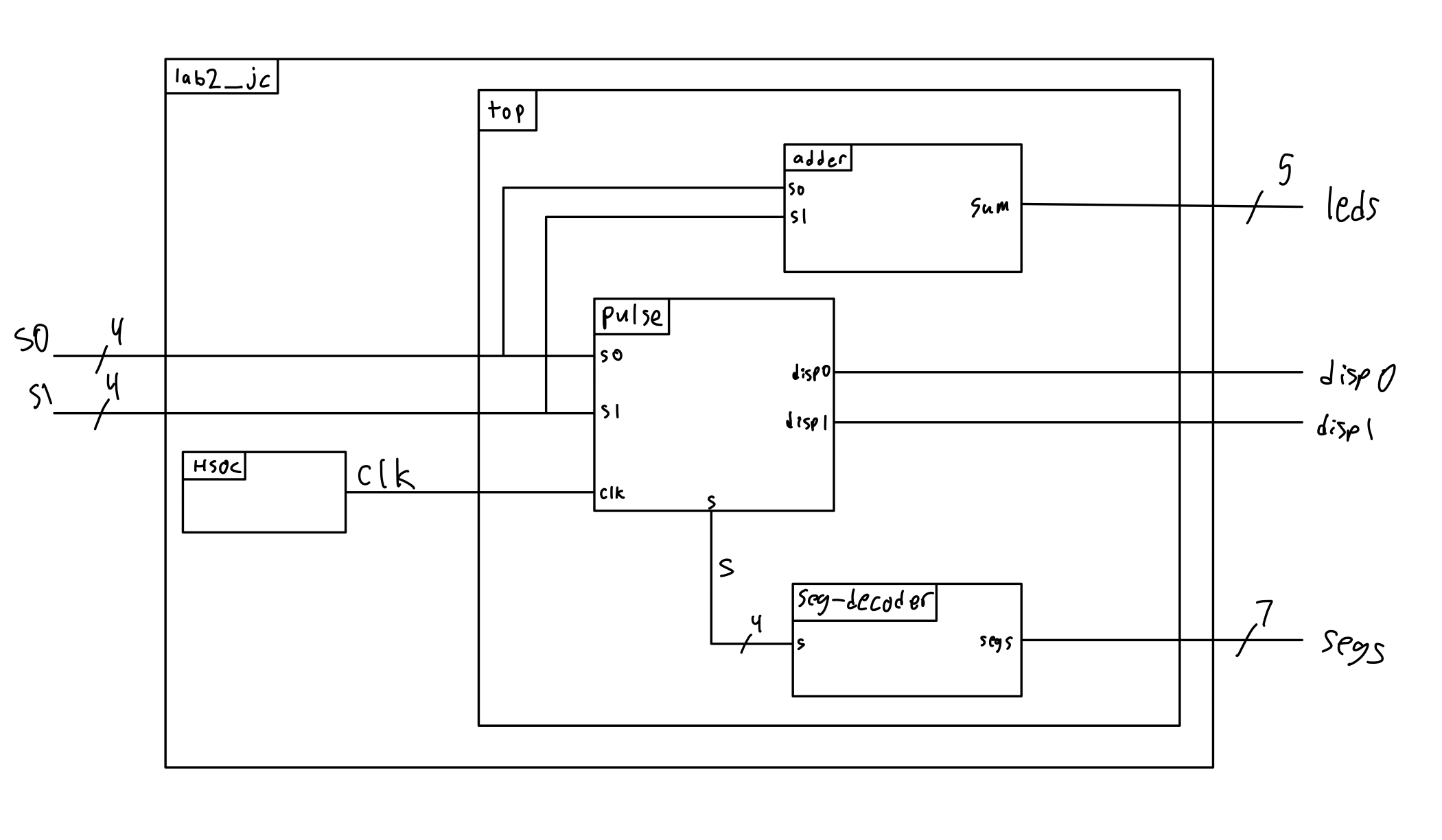
The overall project was broken up into several smaller Verilog modules. A simple adder and the 7-segment display decoder from Lab 1 were combined with a new pulse module that contained most of the logic. The pulse module takes both sets of switches as inputs and, using a counter to produce a slower clock, alternates which set of switches is sent to the 7-segment decoder. It also ensures that the appropriate anode is activated.
The physical design was setup to ensure that the maximum current from the FPGA pins was not exceeded, which necessitated the use of transistors to drive the 7-segment displays.
The Verilog modules were tested using a testbench that applied testvectors covering most corner cases (extremes in this case) along with several other random vectors. It did not seem necessary to test every possible input combination as that number quickly explodes. The physical design was tested using a wide variety of different possible inputs.
Technical Documentation:
The source code for the project can be found in the associated GitHub repository.
Block Diagram

The block diagram in Figure 1 demonstrates the overall architecture of the design. The various modules are described here:
| SystemVerilog Module | Description |
|---|---|
lab2_jc |
FPGA specific module, includes high speed oscillator module |
top |
Top-level, non FPGA-specific module |
seg_decoder |
7-segment display decoder |
pulse |
Rapidly switches which digit of the display is active |
adder |
Computes the sum of the two inputs |
Schematic

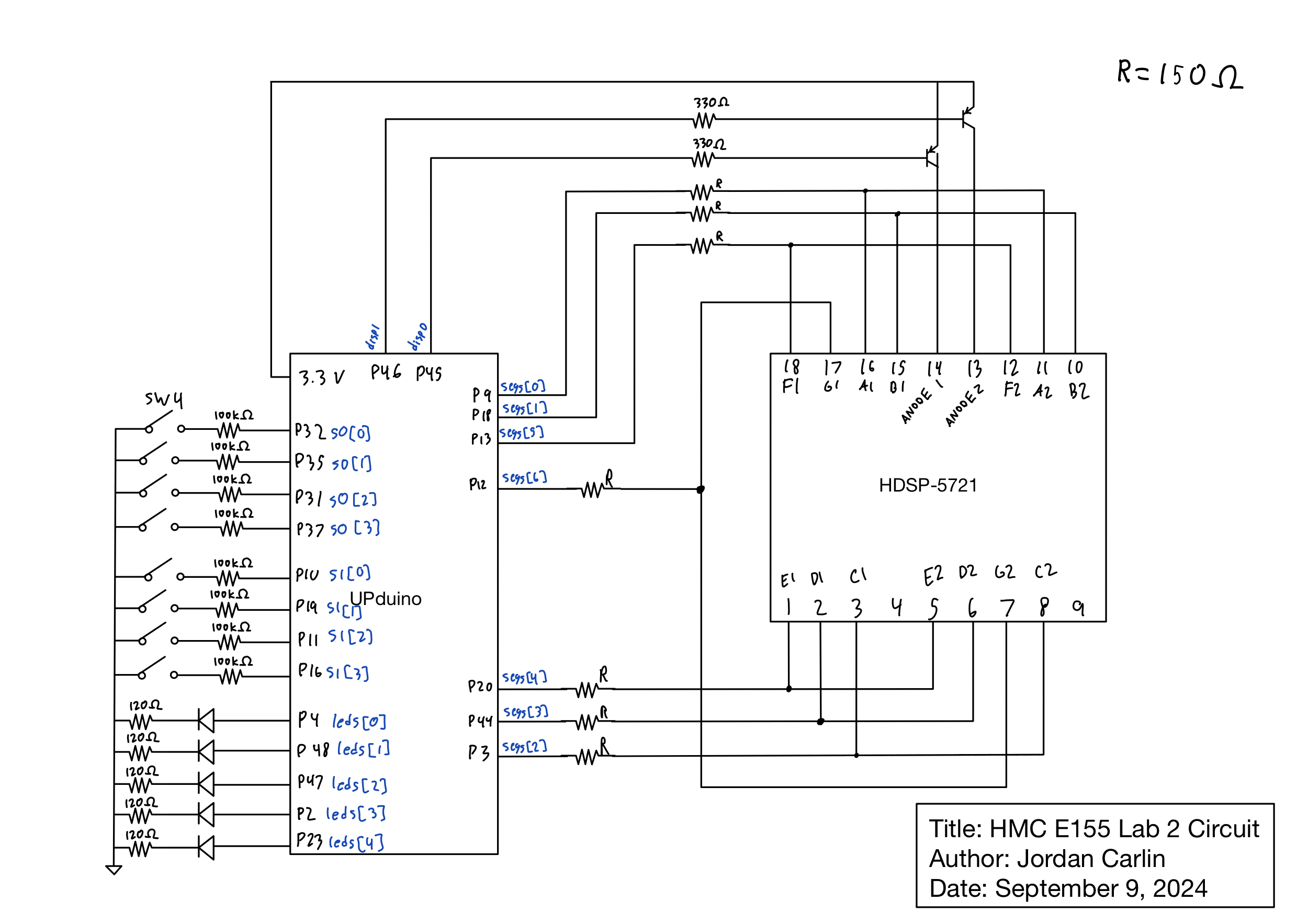
Figure 2 shows the physical layout of the design.
- An internal 100 k\(\Omega\) pullup resistor was used to ensure the input switches were not floating.
- The transistors were connected to the FPGA through a 330 \(\Omega\) current-limiting resistor to ensure that they didn’t pull more than 8 mA, the maximum the FPGA I/O pins can supply (see table 4.13 of the FPGA datasheet). Per their datasheet, the transistors have a voltage drop of 0.65 V, so 330 \(\Omega\) works perfectly based on Ohm’s Law.
- The LEDs in the 7-segment display have a voltage drop of 2.1 V (datasheet), so a current-limiting resistor of 150 \(\Omega\) limits the current through the FPGA to 8 mA.
- The output LEDs for the sum have a voltage drop of 2.35 V (datasheet), so 120 \(\Omega\) current-limiting resistors were selected.
Results and Discussion
Testbench Simulation

Figure 3 shows a screenshot of the QuestaSim simulation validating the Verilog. The physical design works when deployed on the FPGA. The design meets all intended design objectives and specifications.
Conclusion
The design successfully displays two digits on the 7-segment display at the same time with only one set of pins by utilizing time-multiplexing. The LEDs show the correct sum for all input digits.
I spent a total of 13 hours working on this lab.