FPGA
FPGA Setup
The FPGA controls a VGA monitor and stores the image to be displayed on the monitor. It receives SPI packets from the MCU (see MCU description for an explanation of the packets) that specify what changes need to be made to the image. The current image is stored in SPRAM on the FPGA. As SPI packets are received, there is a block of logic on the FPGA that checks what type of data the packet contains (position or color/brush status) and, if necessary, updates certain pixels in the SPRAM accordingly.
The FPGA also has a separate block of logic to drive the actual VGA display. This component scans through each pixel in the SPRAM and sends the appropriate RGB values to the VGA monitor. The pixels are stored in a 3 bit encoding format (one value for each of the 7 colors supported by the system) and a decoder is used to convert these values to the actual 12-bit RGB values for the VGA monitor. The playable area of the screen is 128x128 pixels, so the SPRAM only contains values for those pixels. All pixels outside of this area are set to black. This section of the logic is also responsible for sending the appropriate H-Sync and V-Sync signals to the monitor so it knows when to start a new line or frame of the image.
Block Diagram

The FPGA design builds heavily upon what was done in Lab 7 in MicroPs. It uses a similar design for the SPI module itself (although the decoder is entirely new). Storing the image in SPRAM is also similar to storing the sbox encoding in a ROM in Lab 7. The most significant new part of this design is the VGA driver itself.
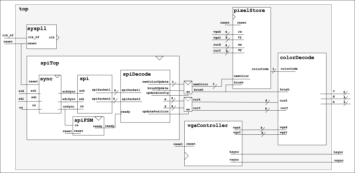
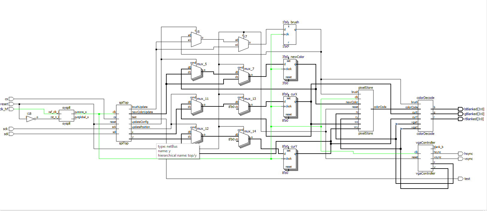
As pictured in Figure 1, many of the modules in this design are heavily intertwined. While ideally each module is a mostly independent thing, the use of the SPRAM makes that impossible for this project. The VGA driver needs to be able to read from the SPRAM, while the SPI decoder needs to write to it. Additionally, the VGA module can not even directly output the RGB values to the monitor because they need to be looked up in the SPRAM and then decoded. The result of all this intermixing means the VGA module sends just the H-sync and V-sync signals out to the monitor, and sends the x and y values to rest of the system for further processing before the RGB values are sent to the monitor. This significantly complicates the timing for the design and makes unit level testbenches difficult to design. The heavily interwoven modules can be seen most clearly in the generated block diagram from Lattice in Figure 2.

Hardware
One of the tricky parts of the hardware design for the FPGA was utilizing SPRAM to store the pixel array. There were many attempts to tweak the Verilog to get the synthesis tool to infer the appropriate block block ram hardware. While this was eventually successful, the block ram ended up being insufficient for the project. Writing to it was too inconsistent, and there were severe timing issues. The final design transitioned to using the SPRAM modules instead, which were able to hold sufficient data and functioned as expected when written to.
The SPRAM was set up to read on every clock cycle based on the x and y values coming from the VGA controller. The current position data and color was always being sent to the write ports, but the write enable line was hooked up to the brush signal to ensure new colors were only saved when the brush was down.
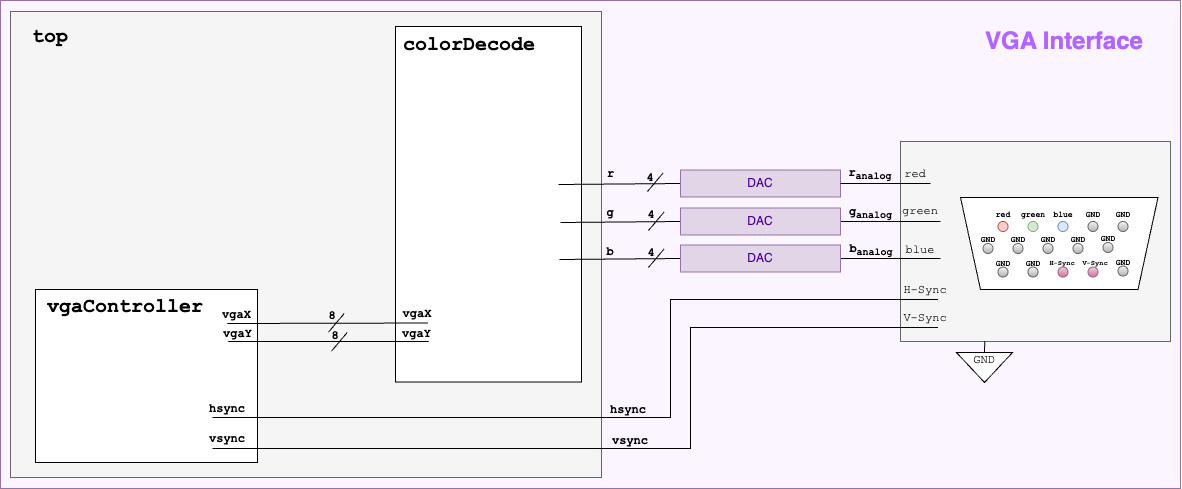
The other main aspect of the hardware design is the actual VGA interface. Figure 3 shows the high-level interface between the FPGA and the VGA monitor. The VGA and colorDecode modules drive these signals, with the colorDecode module driving the R, G, and B signals and all of the timing and sync signals coming from the VGA module.

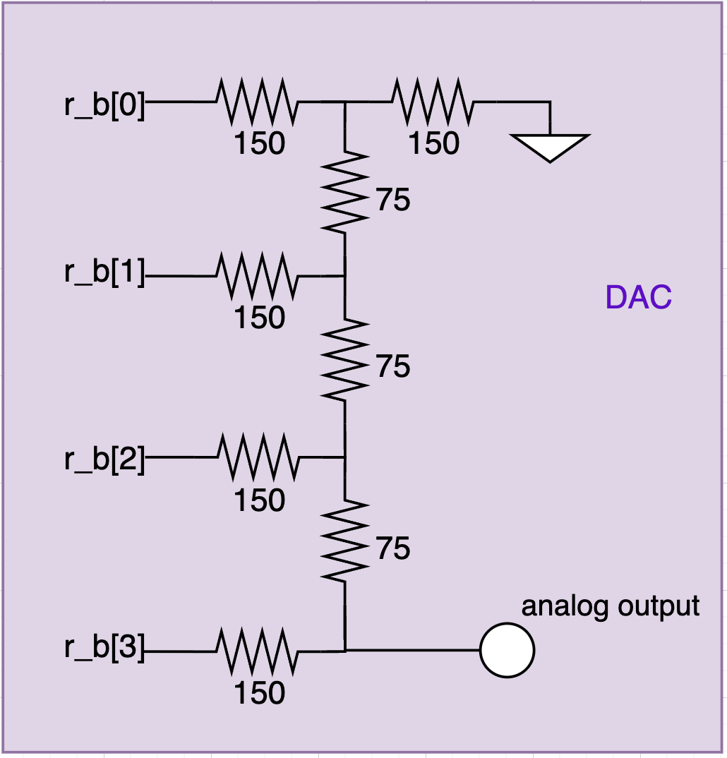
The colorDecode module itself outputs a total of 12 outputs; three sets of four signals for each of R, G, and B. Each set of four digital output pins is put through a digital to analog converter (DAC), which takes advantage of Kirchoff’s Law and the innate 75 Ohm termination impedance of the VGA monitor. A schematic of the DAC can be seen in Figure 4.

This DAC effectively produced a signal between 0 and 0.7 Volts, which could then be sent out to the VGA, which uses the Voltage to generate the appropriate color.