Results
Quantitative Results
The initial goal for this project was to achieve the following:
- Build a system that is able to draw using a joystick controller
- Allow the user to chose between 7 colors to draw with
- Give the user control of the brush’s width (i.e. configure some sort of thickness for the brush)
- Allow the user to pick the brush “off the page” while drawing
- Stretch Goal: A countdown timer that updates every second
Of these initial goals, we achieved enough for proficiency, but were unable to meet our final specs for the countdown timer. Particularly because of the short at the end, during demo day it was additionally impossible to provide user input.
Overall, we achieved almost all of our goals, and likely reached about 90% of what we wanted to achieve in this project. It was just the final small details that got in the way.
Timing
Speed of the MCU
The MCU of the Micro P(ictionary) game used the SystemClock (which runs at 4 MHz) for all calculations.
The analog to digital converter on the MCU relies on the output of the AHB Clock. For further details, view the linked clock tree image in the Appendix. This clock ran at at the SystemClock’s speed during this project.
A new set of modules, STM32L432KC_ADC.c and STM32L432KC_ADC.h, were constructed in order to make for easy initialization of any new ADC pins. The conversion rate of analog to digital signals was not integral to the performance of the system, as we did not anticipate that user would be changing inputs faster than 10 Hz.
The main timing constraint on the MCU side was the sending rate of the SPI. The device is set up to send a new SPI update every 500 ms, based on Timer 12 of the MCU. Because the FPGA would immediately update as soon as it receives its new X and Y direction, the “send rate” of the FPGA also determines the speed with which someone could move the brush on the screen. It was found that the ideal speed to move the brush was 500 ms, but if desired in the future it may be possible to add a potentiometer that increases or decreases the pause time between each update to the brush’s location.
Speed of the FPGA
The FPGA used a PLL to generate a 50.35 MHz clock derived from the main 48 MHz clock coming from the high speed oscillator. This very specific clock frequency was necessary to accurately generate the H-Sync and V-Sync signals for the VGA monitor. The screen was 800 clocks ticks wide and 525 clock ticks tall, but only 640 by 480 of those are usable pixels. In order to achieve an overall refresh rate of ~60 Hz (which is what the monitor expects), the H-Sync signal needed to run at 31.470 kHz, the V-Sync signal at 59.94 Hz, and the RGB values needed to refresh at 25.175 MHz. While this could all be achieved using a clock speed of 25.175 MHz, the PLL was set to run at double that speed to allow for reads and writes to the SPRAM to occur on alternating clock cycles. This means the VGA RGB values were still changing at 25.175 MHz, but the clock signal was running at 50.35 MHz.
Qualitative Results
Analog Pins
The MCU’s use of analog pins was done extremely quickly, in large part thanks to much of the previous work done by past students in Micro P’s. We found the following two sources particularly helpful:
- Camera by Kavi Dey, Henry Merrilees, and Neil Chulani
- Digital Synthesizer by Kevin Box and Eli Rejto
The analog pins were capable of measuring the voltage output of the joystick and the potentiometer. It appeared that, especially towards the end, there were conflicts between the sampled data for x, y, and t, with one of the values consistently outputting significantly higher than expected. The analog output of the pins normally measured their input voltage times 1000 when measured correctly. For example, 3.3 volts appeared as 3300 on the board.
SPI
The design was capable of sending two different kinds of SPI packets: either a color bit packet, or a location packet. The color packet was encoded such that it contained configuration bits 111 at the beginning, which could never be reached by x or y location packets because it exceeded the array range being used (Figure 1 and Figure 2).


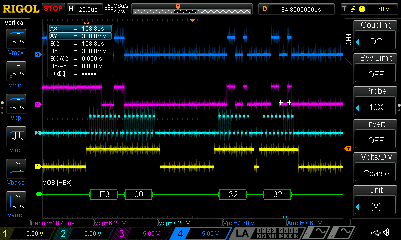
The system was confirmed to be transmitting via SPI early on during the Mid-semester check-in using oscilloscope traces:
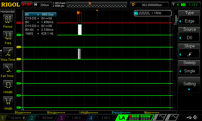
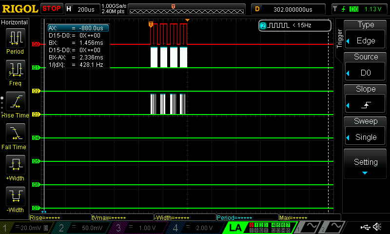
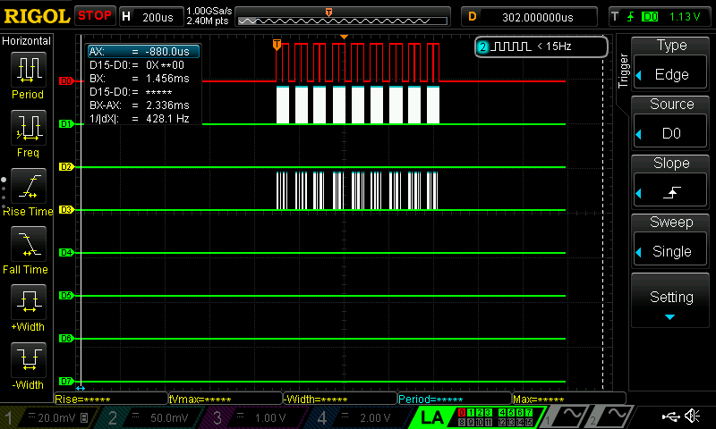
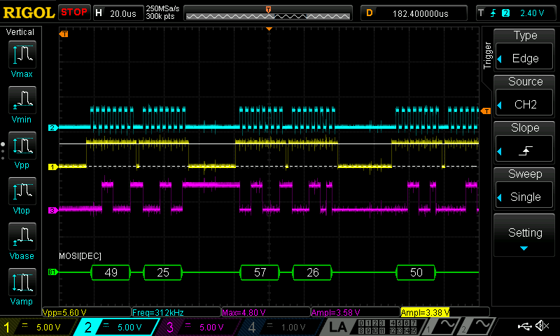
We needed to confirm that the FPGA was properly reaching its desired states based on the incoming SPI packets. This was confirmed using oscilloscope probes attached to the incoming SCK, MOSI, and CS channels and a TEST output pin from the FPGA.
In a method similar to that seen in the following images, various states that the FPGA was able to decipher were output to the test pin to check that the SPI packets were being properly received and interpreted.
All images are encoded such that Channel 1 is CS, Channel 2 is MOSI, and Channel 3 is SCK.
VGA
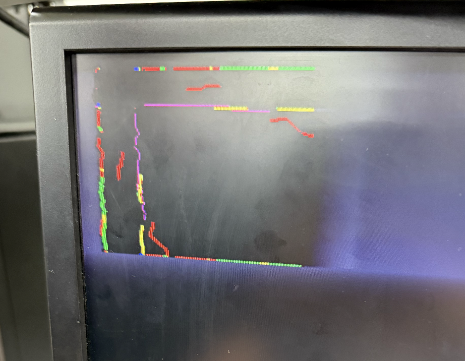
The final system was able to raise the brush up and down, change its color, and move around the screen. From the limited testing that we were able to do, the brush thickness control also appeared to be working. The output image is able to consistently update depending on the color and location inputs. As can be seen in Figure 5, the system was able to create and draw desired images.
Debugging
The following videos show the process of bringing the VGA system out of simulation into the real world.
First, the FPGA was able to output a single hardcoded pixel to the VGA monitor. This version, as we later discovered using the Netlist feature in Lattice Radiant, did not use RAM.
After this, we began trying to set the values dynamically according to what was received via the decoded SPI location packets. We confirmed that the write position coordinates (wx and wy) were correct in simulation by checking that when wx and wy were at a set value, for example 100 and 100, and set to 0'b001 (encoding for red), the RAM was recording that value. This was confirmed within the MemoryList feature of ModelSim.
However, while displaying this on the screen we ran into an issue; the RAM was not being correctly indexed by the system. It was only possible to alter pixels directly using an address in the matrix.
wx and wy bits at a specific section; these bits should be the color that is stored for a specific location, but when they are sent into the array they don’t update correctly, resulting in the oscillating pattern seen above.
This can be seen in Figure 8, where we tried to set the data within the file to wx and wy while reading out the values. For as of yet still unknown reasons, the data was not being correctly indexed by the RAM. The read logic seemed to be working when the RAM was preloaded, which seemed to indicate the problem was with the write logic, but we were unable to determine the exact cause of the issue.
As a result, we moved onto using SPRAM instead instead of the block RAM. SPRAM required that we double the clock speed, but at the same time permitted for better control of what we were sending and receiving to the screen and appropriate updating of the data stored in the RAM. This is where we began to see more expected results.
Figure 9 is a demonstration of color being transmitted correctly. With the confirmation of SPI working from earlier, this video confirmed that we were updating colors correctly based on the data received from the MCU. Our next steps involved filling the entire screen with this data rather than just the noise present in this video.
Figure 10 was confirmation that we could control every bit we wanted to using a write x and y of our choosing. From there, it was just a small change to begin moving the pixels about the board with details sent using the other packet for xy bits.
The Build
Our Final project was made using several bread boards, as well as several laser cut components that give it a finished look. These parts were a breakout board with several color buttons, as well as a casing for a joystick, switch, and potentiometer system.
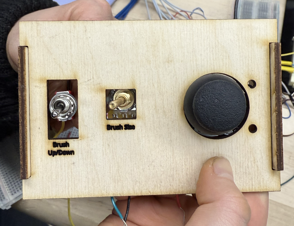
The joystick circuit as well as the circuitry necessary for the VGA was soldered onto a small protoboard to prevent noise and avoid messy wiring.
All seven buttons were put onto a separate bread board to ensure proper circuitry, and were wired in long distance to prevent complex wiring.
The switch and the potentiometer were both free floating, but have been given housing that provides easy control for the user when the design is working.
Final Updates
Unfortunately, near the very end of the project something went wrong with the physical hardware and the MCU was no longer able to receive data from any of the inputs, digital or analog. This meant that the system was no longer able to take any user input, so drawing was unfortunately no longer possible.
The inputs were working until an hour or so before the deadline for this project. Despite them being broken for the actual checkoff, all of the MCU to FPGA communication via SPI and FPGA to VGA monitor communication was working. As a result, images could be displayed as expected. We decided to turn the final version into a “glorified screensaver” for demo day.
The MCU would randomly generate x and y locations and colors, and from there the rest of the chain would proceed as normal: the MCU encoded the data into SPI packets and transmitted them to the FPGA, which then decoded them, updated the SPRAM, and displayed the constantly changing image on the VGA monitor.